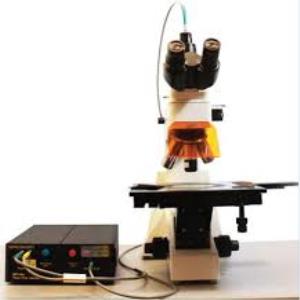
MProbe 40 series
Thin Film Measurement
| 측정 방식 | 비 접촉식 측정 |
|---|---|
| 측정 범위 | 1nm ~ 1000µm |
| 정 밀 도 | 0.1Å or 0.01% (greater of) |
| 빔 크 기 | < 4 µm |
| 응용 분야 | Patterned wafers, MEMS, other samples that require small measurement spot. |
| Practically any translucent or low-absorbing film can be measured: SiO2, SiNx, DLC, Photoresist, Polymer, Polyamide, polySi, nanocrystalline Si, aSi, Si, Parylene, industrial coatings. | |
| Thin-film solar cells: aSi, CIGS, CdT, TCO | |
| Semiconductor and dielectric materials (Photoresist, oxides, nitrides, OLED stack) | |
| Optical coatings (Anti-Reflection, Hard coatings, Filters) | |
| Liquid Crystal displays (Cell Gaps, ITO, Polyamides),Magnetic media, laser mirrors, thin metal films | |
| 첨부1 | 카다로그 |
The MProbe 40 is a complete thin-film measurement system. Select
the model and options the fit best for your application requirements or let us know
your application and we will help to select…
You’ll be ready to start measurements -everything is included.
Our extensive materials library has
500+ materials, with easy import/creation of the new
materials and support for a wide range of parametrized materials (from Cauchy
to Tauc-Lorentz) is included.
One-click measurement combines data acquisition (reflection or
transmittance spectrum) and data analysis. Everybody is a measurement
expert with MProbe!
Of course, we have all the sophisticated tools including
sensitivity analysis, error-estimator, simulation, filmstack switching, global
optimization, x-x-x-x-x-x-x-x-x-layers and materials linking, etc. for complicated applications
development
Reflectance and transmittance spectral data can also be used as a
raw measurement (for example, as in spectrophotometer) or a for a wide range of
other applications.
What’s in the box?
·
Main unit: includes spectrometer(s), light
source (UV models) , electronics (50W halogen light source is included in
microscope
illuminator)
·
Fiberoptic probe
·
Upright inspection microscope with four
long WD objectives-95 mm parfocal length (UV and NIR models have three
visible
and one UVVisNIR achromatic 8x objective)
·
TFCompanion -R software Advanced version
(USB dongle (license key), Software, user guide and other materials on USB
memory stick )
·
Calibration sample (Si or Al depending on the
model) and black absorber pad
·
Test sample- 200nm oxide wafer
·
USB cable (connecting main unit to
computer)
·
Universal power adapter (110V/220V)
In addition, MProbe includes the
following Semiconsoft advantages:
·
Library with over 500 materials and support
for parameterized materials
·
12 months of free software updates and
application support
· Hardware upgrade program
Why use MProbe 40
Micro spot: measure with spot size < 4 µm
Flexible: select the best hardware configuration for your
application. MProbe model and options. Already
have microscope? We can help to integrate…
Affordable: up to 50% savings as compared to other commercial
instruments
Precision: unmatched precision <0.01nm or 0.01%
Materials database: extended database (500+ materials) is included
Software: flexible, user friendly and powerful software; integrated
control/data acquisition and data
analysis;
any filmstack: no limits on number of x-x-x-x-x-layers, support inhomogeneous and thick
incoherent
x-x-x-x-x-layers, surface roughness, multi-sample analysis, etc.
Technical support: application and technical support
Applications
Patterned
wafers, MEMS, other samples that require small measurement spot,
Practically
any translucent or low-absorbing film can be measured: SiO2, SiNx, DLC,
Photoresist, Polymer,
Polyamide,
polySi, nanocrystalline Si, aSi, Si, Parylene, industrial coatings.
1nm-1000µm
thickness range
Thin-film
solar cells: aSi, CIGS, CdT, TCO
Semiconductor
and dielectric materials (Photoresist, oxides, nitrides, OLED stack)
Optical
coatings (Anti-Reflection, Hard coatings, Filters)
Liquid
Crystal displays (Cell Gaps, ITO, Polyamides)
Magnetic media, laser mirrors, thin metal films
![]()
![]()
![]()


